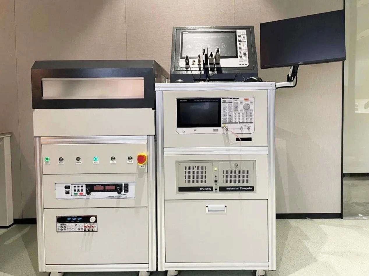
Power Device Dynamic Parameter Test System
Provides comprehensive characterization of static parameters for high-power devices, and supports fully automated capacitance measurement under high-voltage bias.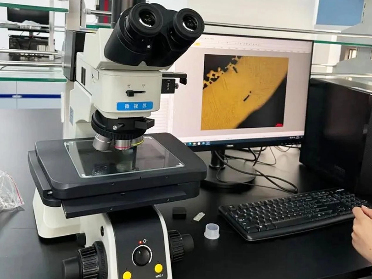
High-Magnification Metallographic Microscope
Supports ultra-deep-focus optical observation at magnifications up to 1000X.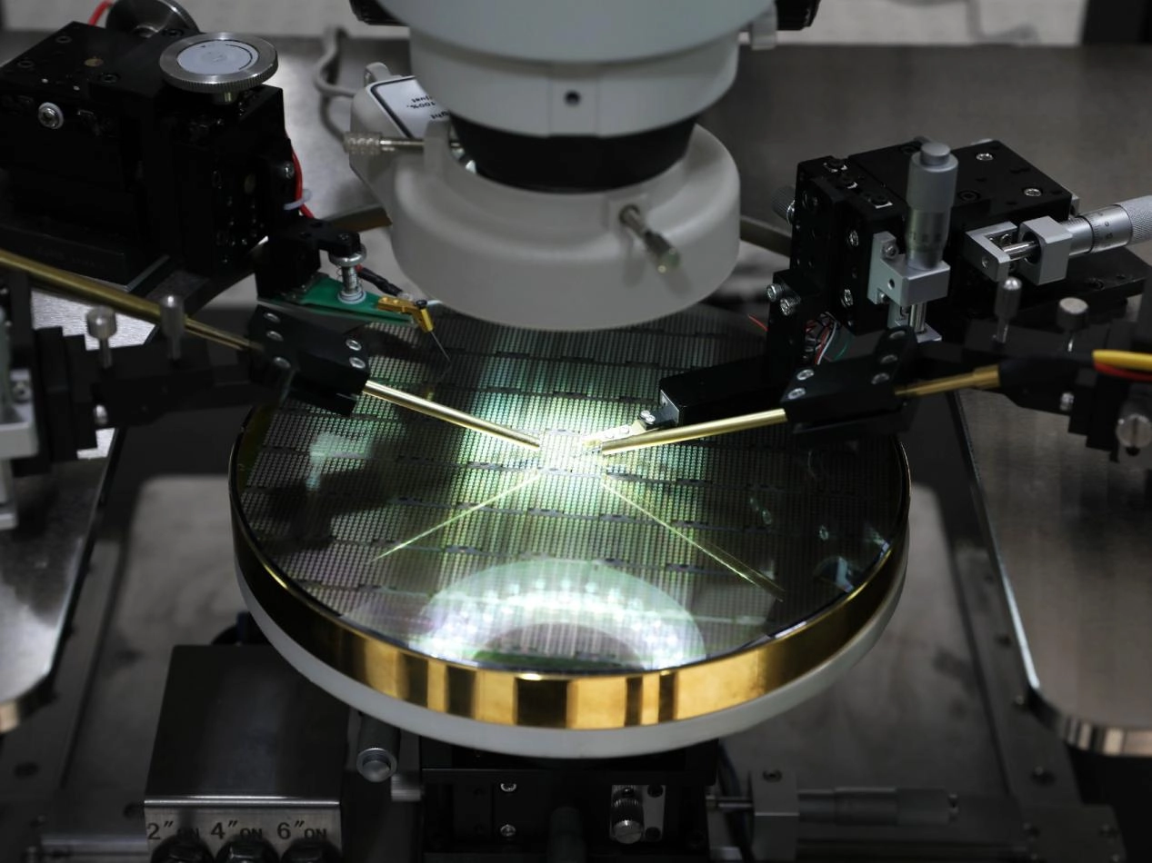
Wafer Probe Station
Dedicated Taiko-process probe station, supporting ultrathin 8-inch wafers down to 60 μm.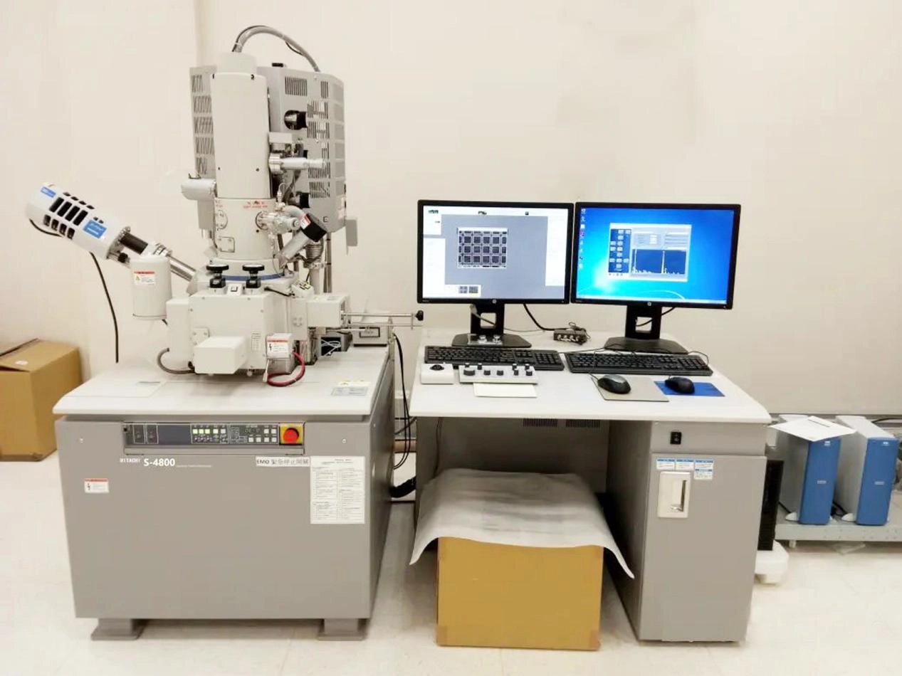
Scanning Electron Microscope (SEM)
Offers magnification up to 300,000× with an integrated energy-dispersive spectrometer (EDS), suitable for micro-area morphology imaging and compositional analysis.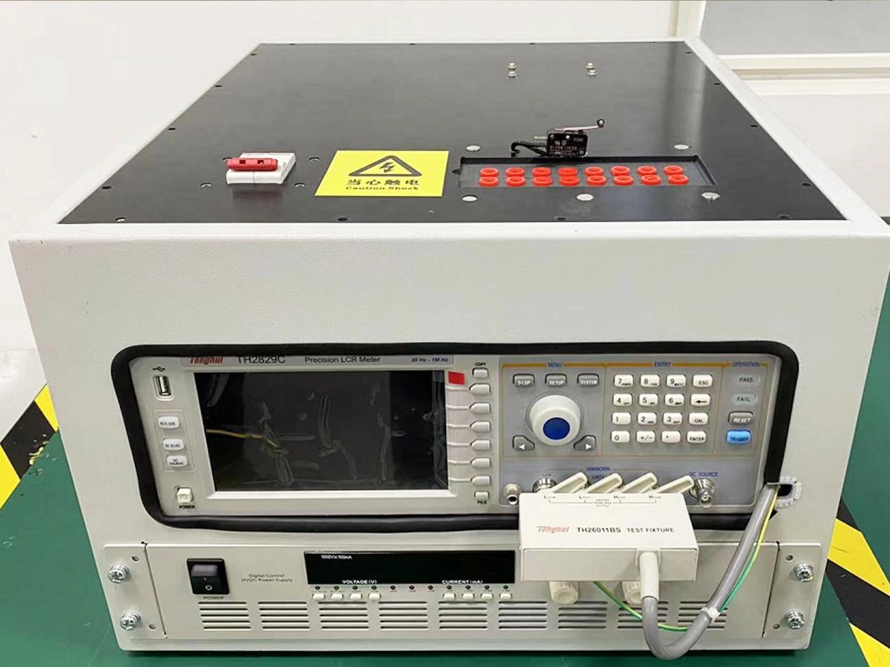
Gate Capacitance & Resistance Tester
Accurately measures the gate capacitance and gate resistance parameters of power semiconductor devices.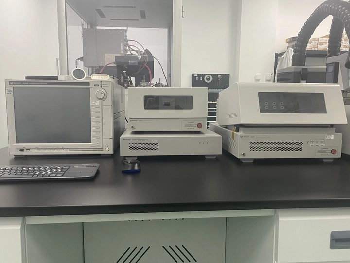
Power Device Analyzer / Curve Tracer
Provides comprehensive characterization of dynamic parameters for IGBT devices, enabling screening of dynamic defects and parameter inconsistencies.